

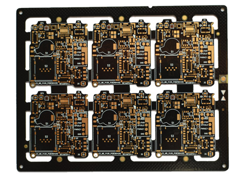
App.:Security Electronics
Thickness:1.0mm
Surface treatment:ENIG+OSP
Material:FR4 TG150
Layer:6L
The manufacture of multilayer board of FPC is in the "core" on the surface of coated or laminated dielectric layer (or resin coated copper foil) and the formation of micro vias and making, these formed in the core plate laminated on micro via in optical method, plasma method, laser method and sandblasting method (mechanical method, including CNC drilling method introduction etc.) and other methods to prepare the multilayer FPC circuit board. These micro vias through hole metallization and electroplating copper to achieve multilayer FPC layer electrical interconnection. This section mainly introduces the characteristics and requirements of micro conductive holes in the FPC board of the multilayer board.
The through hole to say, if the vertical hole plating, through the multilayer FPC circuit board plating fixture (or rack) swing, vibration and bath stirring or a jet flow method of multilayer FPC hydraulic difference in plate two between the surfaces, the pressure will force the plating the liquid into the hole and get rid of the gas in the holes and full in the hole, for the high aspect ratio (the ratio of radius to thickness: the thickness of the dielectric layer and micro conduction aperture ratio) of the micro hole, the hydraulic pressure difference is more important, then the hole or plating. In the hole of electroplating, all need to consume the part of the Cu2+ ion in the hole, so the Cu2+ concentration in the hole is getting lower and lower, the efficiency of the hole or plating will become smaller and smaller. The effect of bath fluid through holes and (as can be regarded as "laminar" phenomenon) and the uneven distribution of current density (the hole density is far lower than the first-class electric current density board), therefore, the thickness of the coating in the hole at the center of the surface of the coating thickness is always less than.
In order to reduce the thickness difference, the most fundamental way: one is to exchange the bath circulation or unit time increase of bath hole inner hole number (assuming a replacement of bath, is actually much more complex, but this assumption is to explain a problem); the two is to improve the current density in the hole, this is difficult, or that it is not feasible, because the increase of current density, bath hole, will increase the current density, the surface in this way, resulting in greater thickness difference between the hole at the center of the coating thickness and surface coating; three is the concentration of Cu2+ ion the current density decrease during electroplating and plating solution, and improve the hole bath circulation (or bath, as a result, the exchange number) can reduce the concentration of Cu2+ ions in the bath surface and hole difference (refers to the part of consumers The difference between Cu2+ and Cu2+ concentration in plating solution consumption change caused by this difference, measures and methods) can improve the surface coating and plating hole (at the center) the difference between the thickness, but often have to sacrifice the multilayer FPC productivity (output) as the price, this is undesirable; four is the use of pulse plating method, according to the different thickness of high aspect ratio micro holes, electroplating method {can significantly improve the FPC surface coating and multilayer board between the hole plating thickness difference by pulse current corresponding to the thickness of the coating, even up to the same. These measures for the multi - plate FPC circuit board in the micro - through hole plating can be applied to it?
As mentioned above, hole plating multilayer FPC circuit board in the micro vias is carried out in the blind hole, when the hole hole depth or small diameter thickness ratio of hours, practice has showed that the four measures of the electroplating can get good effect.
However, when the blind hole depth high aspect ratio or large, micro conduction hole plating reliability? Or, how to control the multilayer circuit board blind hole depth or diameter thickness ratio of the appropriate level?
As for using the horizontal hole plating multilayer FPC circuit board in the microvia case no detailed reports, but people can imagine, for multilayer FPC board thickness to diameter ratio is small, using horizontal hole plating should be able to get the electrical interconnection reliability. For the larger diameter thickness ratio of blind vias, multilayer board FPC of the lower surface of the blind via hole is difficult to get rid of the gas in the holes, even the bath in the holes are difficult, not to mention the bath exchange in the hole, unless the Board regularly flip. According to the hole, electroplating characters and basic principle of FPC circuit board above the multilayer board, we can conclude that using the horizontal hole plating multilayer FPC circuit board blind via hole (especially thick diameter ratio, such as the ratio of thickness to diameter is less than >0.8) vertical hole plating.